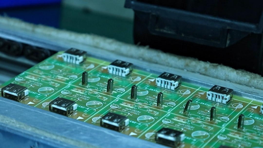
In recent years, semiconductor technology has seen unprecedented growth and innovation, driven by the insatiable demand for higher computing power, improved efficiency, and energy optimization. From powering smartphones and autonomous vehicles to fueling the servers behind artificial intelligence and cloud computing, chips are the silent workhorses of our digital age. In this article, we delve into the latest breakthroughs in chip design and manufacturing that are setting the stage for the next generation of technologies.
TLDR: Semiconductor technology is advancing at a rapid pace, with innovations like 2nm process nodes, chiplets, and AI-integrated designs reshaping performance capabilities. Companies such as Intel, AMD, TSMC, and NVIDIA are leading breakthroughs that will transform industries ranging from consumer electronics to aerospace. Energy efficiency, scalability, and customized architectures are emerging as the top priorities. These advancements promise faster, smarter, and more sustainable computing across the board.
The Shrinking of Transistors: Moore’s Law Continues
One of the core truths of the semiconductor world has long been Moore’s Law, which posits that the number of transistors on a chip doubles approximately every two years, leading to exponential growth in computing performance. While many predicted its end due to physical limitations, recent breakthroughs have breathed new life into this law.
Most notably, the development of 2-nanometer (nm) and even early 1.4nm chip fabrication technologies marks a major leap forward. Companies like TSMC and IBM have pioneered these advanced process nodes, allowing billions of transistors to fit into a single chip the size of a fingernail. This enables faster speeds, lower power consumption, and significantly better heat management.
Key benefits of smaller process nodes include:
- Lower energy consumption: Critical for mobile and edge computing.
- Higher processing speed: Ideal for AI and real-time applications.
- Increased transistor density: More functionality on a single chip footprint.

These developments are not purely academic. IBM’s 2nm chip prototype, unveiled in 2021, demonstrated 45% better performance and 75% lower energy use compared to 7nm chips. TSMC, the dominant foundry leader, has announced volume production of 2nm chips for consumer-ready products in 2025. The race to define the 1nm barrier is actively underway, a testament to the relentless pursuit of miniaturization.
The Rise of Chiplet Architectures
As traditional monolithic chip designs become difficult to scale, the industry is embracing a new paradigm: chiplets. These are modular pieces of silicon that can be mixed and matched to create a larger system-on-chip (SoC) or multi-chip module. This approach introduces unprecedented flexibility and performance benefits without pushing fabrication limits.
AMD has been a trailblazer in this space, utilizing chiplet-based architecture in its Ryzen and EPYC processors. Intel, too, has committed to chiplets with its Ponte Vecchio GPU and upcoming consumer processors.
Advantages of chiplet architectures include:
- Improved yield: Smaller chips are less likely to have manufacturing defects.
- Scalability: Different chiplets can be designed with varying functions and fabricated using optimal process nodes.
- Cross-vendor compatibility: In the future, chiplets from different manufacturers may be integrated together.
This shift is also fueling the development of interconnect technologies such as Intel’s EMIB and AMD’s Infinity Fabric, which allow individual chiplets to communicate at blazing-fast speeds with negligible latency.
AI at the Silicon Level
Artificial intelligence is not just a user of computing resources anymore—it is becoming part of the chips themselves. New processors are being specifically designed to accelerate AI workloads, incorporating dedicated circuits called NPUs (neural processing units) or AI engines.
Apple’s M-series chips integrate machine learning accelerators capable of 15 trillion operations per second. NVIDIA’s Grace Hopper Superchip is designed specifically to combine GPU and CPU capabilities optimized for AI and high-performance computing. Likewise, startups like Groq, Cerebras, and Graphcore are creating purpose-built AI chips that operate at incomparable efficiency levels for deep learning models.
These chips are tailored for applications such as autonomous driving, voice recognition, and predictive analytics. The move toward AI-designed chips (using AI to design better semiconductors) is also starting to surface, with tools from Synopsys and Google leading the way in automated circuit design.
Energy Efficiency and Sustainability
Semiconductor manufacturing and chip performance are increasingly scrutinized for their environmental impact. Newer chips are being engineered to balance raw processing power with energy efficiency to reduce carbon footprints across data centers, personal devices, and smart appliances.
Companies like Intel have committed to carbon-neutral manufacturing by 2040, while TSMC plans to use 100% renewable energy by 2050. From advances in material science—like using graphene and gallium nitride instead of silicon—to leveraging 3D stacking for thermal efficiency, the chip industry is marching toward greener horizons.
Technologies driving energy optimization:
- 3D integration: Reduces distance between circuits, cutting transmission losses.
- Power gating: Shuts down idle sections of the chip to save energy.
- Dynamic voltage scaling: Adjusts power based on workload demand.
The Role of Specialty Chips: Customized for Function
Alongside general-purpose CPUs and GPUs, the need for specialized processors—known as Application-Specific Integrated Circuits (ASICs) and Field Programmable Gate Arrays (FPGAs)—is growing in fields like cryptocurrency mining, 5G infrastructure, defense, and space exploration.
Google’s Tensor Processing Units (TPUs) are optimized for AI training processes and are a successful example of in-house custom IC development. These chips deliver significant improvements in inference speed and training time while reducing energy requirements.
The continued expansion of the Internet of Things (IoT) and demand for real-time analytics at the edge is also driving the adoption of tiny, efficient chips tailored to singular tasks with strict power and latency constraints.
Challenges on the Horizon
Despite these remarkable advancements, the semiconductor industry is not without its hurdles. Chief among them are:
- Global supply chain instability: Chip shortages in 2020–2022 revealed the fragility of global manufacturing networks.
- Fabrication costs: Building a state-of-the-art fab costs upwards of $20 billion and takes years to complete.
- Design complexity: As chips become more capable, their design and verification processes grow exponentially more difficult.
In response, governments are intervening. The U.S. CHIPS Act and the EU Chips Act are examples of multi-billion dollar initiatives to restore domestic manufacturing capacity and ensure supply chain resilience.
Conclusion: An Era of Co-Design and System Thinking
Gone are the days when faster chips alone determined product superiority. The new approach is co-design—where hardware and software are developed synergistically to optimize performance, energy use, and functionality from the ground up. Semiconductor innovation is no longer isolated to fabs and labs—it is a strategic imperative across industries and nations.
As we look ahead, the semiconductor landscape will be characterized by a mix of decreasing nanometer sizes, increasing architectural complexity, and a growing emphasis on sustainability and customization. Whether enabling next-gen smartphones, revolutionizing AI, or fueling space exploration, the new age of chips is central to progress in the 21st century and beyond.
